 Now that I know a couple of ways how to build a clock generator I've moved on to the next step and have started looking into what kind of RAM I want to use for my Do It Yourself CPU (DIY-CPU). Here's the story of how that went:
As it's an experimental system I only need a couple of bytes of RAM to hold a short program and a few bytes of data. I don't want to build it myself, however, as I feel confident that I understand how static RAM is composed of flip-flops, how flip-flops are built with gates and why they have two stable states. Therefore I had a look around for a small off-the-shelf RAM chip that I can.
The smallest static RAM chip I could find has a size of 8 kilobytes which sounds very little by today's standards of course. However, that is far beyond what I need anyway, I would have already been content with a 256 byte version. Anyway, so I bought an 8 kB CMOS RAM chip and for those who'd like to take a closer look you can find the datasheet of the WS6264 here.
To get a feeling of how I can write data into the chip and get it back out again I used a breadboard to experiment a bit. To make life a bit easier I decided not to use physical switches and LEDs to control and read data from the address and data buses. Instead I decided to use a Raspberry Pi with a Pi-Face extension board that offers 8 digital inputs and 8 digital outputs and the flexibility of Python programs to read and write data on the various pins of the RAM chip. As 8 inputs and 8 outputs are obviously not enough to control all of the 8 address bus pins, the 8 data bus pins and the various enable and set lines I had to simplify a bit and only use 3 bits of the address bus and 3 bits of the data bus and grounding all other lines. In other words I limited myself to reading and writing 2^3 = 8 bytes. More than enough to get a feeling for how to read and write data into the chip. In addition to the bus pins I also control the Output Enable line and Write Enable line of the chip with two output ports of the Raspberry Pi.
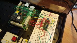
The first picture on the left shows this setup. The green cables between the breadboard and the Raspi go from the RAMs first three data bus pins to three input ports of the Raspi so I can monitor the data bus. The forth green cable is the common ground. The red cables between the Raspi and the RAM are the first three address bus pins that I can control with 3 output port pins of the Pi. The orange cable connects to the Write Enable line and the yellow cable connects to the Output Enable line.
To write something to a memory location I used a little Python program to put the address over the red cables on the address bus. The red button that can bee seen at the bottom of the image is used to set one of the 8 bits of the byte to either 0 or 1 while all other bits of the data bus are pulled to ground. This way I can cycle through the 8 bytes I can address and set one of the 8 bits to either 0 or 1 while all other bits are always 0. Remember, it's only to figure out how things work so there's no need to set all 8 bits of the byte. Just seeing that the bits come out correctly again later on is enough.
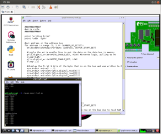
 Once the address is on the address bus and I have either pressed the button or not to write a 1 or 0 respectively to one of the bits I activate the Write Enable line for a short time (by pulling it to ground) and release it again to commit the value to the chip. With a loop in the Python program I then go to the subsequent memory addresses and repeat the exercise seven more times. In a second loop that follows I cycle through all addresses again but this time I use the Output Enable line to put the stored data on the data bus and read it's values via the Pi-Faces input ports and display the result in a console window and also on the graphical simulation in the exported GUI as shown in the second figure on the left.
It took a couple of hours to get everything working but in the end I managed to figure out how to use the control lines to write and read my bits. Every day, I must read and write billions of bytes to a RAM chip by working with computers, smartphones and other devices. But that's something that happens in the background without me consciously doing it. With this experiment I have physically written and read bytes to and from memory by hand for the first time in my life. Quite an interesting thought 🙂
Also, I figured out how to pull the data bus lines to ground via 33k Ohm resistors so I can use the lines for both input and output which will be required in the next step when I hook up a number of other components such as registers to the bus that will be part of the CPU so I can transfer CPU instructions and data between them and the RAM chip. The order for the additional chips has already gone out and I will soon report how that went.