Microcode Implementation In A Real Processor

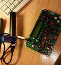
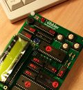
One of the biggest revelations I had during my (ongoing) journey to discover how a processor really works is to find out how that mystical microcode in a CPU is implemented. Things culminated in the 4-Bit Nibbler Do-It-Yourself CPU project that uses a microcode ROM in the control part. For understanding how microcode works it can’t get much better than that. Except…

Continue reading Microcode Implementation In A Real Processor

The DIY Retro Game Console Revisited

retro-not-assembled-smBack in December I returned from 32C3 with a DIY retro game console kit created by Voja Antonic as it promised to be fun to assemble and to study the source code. To me it was “the” hardware discovery of the congress! Apart from the prospect of playing a retro-game and to feel transported back into the 1980’s I was intrigued by the fact that the VGA graphics is not generated by a dedicated graphics unit but is instead done in software on the PIC CPU with three digital outputs that are connected to the red/green/blue lines of the VGA connector and two additional digital outputs to drive the horizontal and vertical synchronization signals for the screen. In other words, a perfect platform to get a hands-on practical view of how bits in memory can be transformed to a colorful picture on the screen.

Continue reading The DIY Retro Game Console Revisited

32C3 – A One Chip Retro Console For Assembly Programming

Voja-single-chip-cpuMy 32C3 discovery of the day: I’m not quite at the end of my Nibbler discoveries yet but I’ve just figured out how I want to continue my hardware adventures by climbing up the CPU ladder just a bit to something with interrupts and a real hardware stack: Voja Antonic’s ‘DIY Single-chip 2D Retro Game Console’!

I’ve already discovered the project a couple of days ago on the 32C3 Workshop page and yesterday I met them by chance in one of the hardware assembly and soldering areas of the Congress. After talking to them for a while I was intrigued enough that I had a look at the assembly code provided online over night. After that I was pretty much hooked…

One thing that particularly grabbed my attention was that the PIC doesn’t have a traditional VGA screen output or graphics unit. Instead, the VGA connector is connected to three D/A converters four digital outputs and an assembly program triggered by horizontal and vertical timings required for the VGA output invoke routines to paint the screen. Great, not only will I stay very close to to the real hardware, this way I will also learn a lot of how a bitmap and moving sprites stored somewhere in memory can be converted into a video signal.

Voja the creator of the board and Milos, who’s organized the BalCCon hacking conference in Novi Sad this year and the presentation of the project at 32C3, thanks very much for coming with this great project. I’m sure I’ll not be the only one who will be massively inspired by this!

The 4-Bit Nibbler CPU and Bitscope for Layer 1 Logic Analysis Fun

Nibbler-bitscope-smAfter a closer look at how to program the 4-Bit Nibbler CPU and how to cope with its intentional limitations it was time to go one step further and have a closer look at how the hardware works one layer further down. To see the signals and how they propagate through the system a logic analyzer is needed with as many inputs as possible to trace digital signals at different places. Unfortunately, most logic analyzers I found are not cheap, costing several hundred euros even for entry level models. Another alternative would have been to buy a cheap clone hardware from China and then use it with software from the original vendor. As I don't think that's fair I never considered that approach either. But thanks to the January 2016 edition of the Linux Voice magazine I stumbled across the Bitscope Micro, a 2 channel low cost oscilloscope and 8 channel logic analyzer that costs around 120 Euros, tax and shipping included. That's quite in the range of what I was willing to spend. In addition they offer their software for Windows, the Mac and also for Linux. In other words, a perfect match for my needs.

Bitscope screenshotThe logic analyzer can sample digital signals at a rate of up to 40 MSamples/s, enough to have a decent resolution for my Nibbler board running at 2.4 MHz. Any channel can be used as a trigger with rising and falling flanks or a high and low signal level so it's possible to capture signals at a specific moment. The picture and screenshot on the left shows the Bitscope Micro connected to the Nibbler and a commented screenshot that shows how instructions are read from the ROM and put into the instruction register two clock cycles later. For the screenshot I used the blinking LED program that just uses 5 instructions to switch the LED on and off again and then jumps back to the beginning of the program. In total that is exactly 10 clock cycles in which the instructions repeat over and over. This way it's easy to find the beginning and the end of the loop when looking at the signal levels. I spent many hours analyzing traces of signals from many different parts to confirm my theoretical knowledge of how the control unit, clock and phase make the system "come alive". A wonderful exercise during which I once again learnt a lot about what makes a computer really tick.

The Nibbler 4-Bit CPU Project – Learn to Love What You Don’t Have – And Work Around It

The Nibbler 4-Bit CPU board is optimized for exactly one thing: Creating a fully functional computer with a CPU split into its components with as few chips as possible to make it easy to build it and to actually understand what is going on. It does an excellent job at this and one can even learn a lot about CPU architecture design from stuff that has been left out of the design on purpose. Here are a couple of examples and how to work around the missing parts:

No stack: Whenever writing a program that does more than just switching an LED on and off it's almost certain that the program will be split up into subroutines or that one uses a library of routines built by others. To be able to jump and return to a subroutine from several places, the current content of the program counter is put on the stack to serve as a return address. In addition, all input variables to be used by the subroutine are pushed onto the stack as well. The subroutine then retrieves (“pops”) the variables from the stack, does whatever it needs to do and then executes a 'Return from Subroutine' CPU instruction. The CPU then puts the return address that was put on the stack back into the program counter which effectively returns to the main program thread. As the Nibbler does not have a stack it's not possible push the program counter and variables on the stack and return from a subroutine to various places with a single instruction at the end of the subroutine. The way to work around this is to implement a jump cascade at the end of a subroutine. Whenever the subroutine is re-used, the jump cascade has to be modified by inserting a new return target at the end. Which jump to take is written into a memory location before jumping to the subroutine. A different value is used from each jump location. In other words, if the subroutine is used in 8 places in the program there is a cascade of cmp/jz instructions at the end of the subroutine. Also, the subroutine has to be modified whenever it's used from an additional location. Not elegant at all but the only way to have subroutines without a stack. To pass variables to the subroutine, they have to be put in memory (the 'heap') at predefined locations. I'm pretty sure if somebody has never ever heard of the 'stack' concept it wouldn't take long to come up with it as it's just a pain to do just about anything without one.

No indexed addressing: One thing computers are good at is to do simple things quickly over and over again. For example, in many cases it's required to make the same calculation on consecutive input data and to put the results back into memory one after each other. Another repetitive thing is to write into a buffer, e.g. writing a string to be sent to the LCD display into a buffer, one byte (or nibble in this case) at a time. An elegant way to do this is to do repetitive things in in a loop by using an index variable to point to the current input parameters and an index variable that points to where the next output in a buffer can be written to. The way this is done on machine instruction level is called indexed addressing. An instruction to write into memory is given a base address to which the content of an index register is added. After writing to memory, the index register is increased by one and the next loop iteration begins. Thing is, there is no index register on the Nibbler and therefore no indexed addressing, again for the purpose of making the hardware as simple as possible. The only way to work around this is to do repetitive things one after another rather than in a loop. If an action needs to be repeated 20 times, no loop can be used. Instead, the same instructions have to be repeated 20 times in the code with different source and destination addresses. Like the return cascades above, the missing functionality produces very ugly code and makes more complicated stuff that requires many iterations over different input and/or output data difficult to implement on the Nibbler.

No hardware interrupts: A great way of checking for external events is to use hardware interrupts. When the CPU notices an interrupt bit being set it suspends normal program execution and automatically sets the program counter to the beginning of a service routine for that interrupt. This makes it easy, for example, to check for the user pressing a key and to react to it immediately without delay. On PCs, hardware (and software) interrupts are used for many things such as for example peripheral devices indicating that data has become available for processing. It should come as no surprise that the Nibbler does not have interrupts. Checking for key input on the Nibbler thus requires polling the single 4 bit input register to detect when a bit connected to one of the input keys changes its state. This has to be done frequently as otherwise there will be a noticeable delay between the user pressing a key and the computer reacting. In programs that use delay loops between activities, checking for key input must be done in the delay loops to avoid this lag.

No add with carry: Another thing that very much simplifies the hardware design but makes life difficult on the software side is that there is no add with carry instruction. Therefore, adding up integers that are comprised of more than a nibble requires saving the carry flag in a variable and checking for it when using the add command on the next nibble. In practice even more work has to be done because a carry bit can result from adding one value to another or from adding the carry bit to a value. Together with not having an index register makes the whole affair quite complicated in practice.

Every instruction executed in two clock cycles: One of the brilliant design choices that significantly reduces hardware complexity is to execute every instruction in exactly two clock cycles. In the first clock cycle the instruction is loaded into the FETCH register and then executed during the second clock cycle. As the first clock cycle has also advanced the program counter the new 8 bits from the program ROM will either be used as the next instruction in case the program counter is not increased during the second clock cycle for the current instruction or as the lower 8 bits in combination with another 4 bits of the current instruction and put on the address bus to use the content of a RAM cell as the second operand in an operation. Very clever but that obviously also limits the complexity of a task that can be done with an instruction. That's why more complex CPUs use a variable number of steps per instruction and a more generic addressing scheme. Needless to say that more hardware would be required for that. And on the other hand there are only 16 instructions anyway so there's little opportunity for making some of them more complex.

Lots of technical detail in this post, perhaps better understood when looking directly at the source code. I've put one of my programs I've done for the Nibbler on Github which goes into the details of all the topics mentioned above. It can be compiled and run in the Nibbler simulator or, of course, on the real hardware.
Running the Nibbler on a 2 Hz Clock – Who Needs 2 MHz Anyway?

Nibbler-2hz-clockNow that the Nibbler hardware is up and running I can go about and modify the hardware a bit. It's cool to have the board running at 2.4 MHz as everything written in assembler for a 4-bit CPU just runs at a breathtaking speed. Who needs GHz's on such a system? While speed is cool it has the slight disadvantage that doing something as benign as letting an LED blink once a second requires massive delay loops. With 4-bit counters it actually requires 4 nested delay loops. No, the board has no interrupts that one could work with as the focus was on reducing the hardware as much as possible while still having a real computer to work with.

As everything about the Nibbler is static, it's possible to turn down the clock rate as low as 0 Hz. For educational purposes I decided to replace the 2.4 MHz clock generator on the board with a 2 Hz clock I assembled out of two Not (Inverter) gates, a capacitor and a resistor. The extra LED and resistor shown in the image next to the Not-gates IC are not really needed as they are just for showing the clock impulses.

At two Hertz, each assembly instruction of the Nibbler takes exactly two clock pulses, or one second. At that rate it's actually possible to count instructions and visualize where the program currently executes. For the purpose I've written a short program with 5 instructions that switches the on-board LED on and off:

; x-2hz-clock-led.asm

; OUT ports
#define OUT_PORT_LED $E ; 1110 – bit 0 is low
 
; =================================================
 
led_blink_loop:
    ; LED on
    lit #0
    out #OUT_PORT_LED

    ; LED off
    lit #4
    out #OUT_PORT_LED

    jmp led_blink_loop

At 2.4 GHz the only thing that can be observed is a constantly glowing LED though not as bright as it could as it's only switched on 50% of the time. At 2 Hz, however, the LED blinks with a frequency of around 1 Hz. When the program starts and the LED is off it takes exactly 4 clock pulses before the LED is switched on because the output port for the LED is only pulled to ground in the 2nd cycle of the second instruction. 4 cycles later the LED is switched off again. It then takes 6 cycles before the LED is turned on again because there's the jump instruction at the end of the program that takes 2 cycles in addition to the two instructions that load the value to be written to the output port into the accumulator (lit #0 = load immediate) and the output command itself that writes the content of the accumulator to the output port.

Counting machine instruction executions with your fingers, when's the last time you did that? 🙂

The Nibbler 4-Bit CPU Project – First Run

Nibbler-first-run-smI you haven’t seen my previous posts on the Nibbler, have a look here for what happened so far.

It’s a November evening which means it’s dark and cold outside and I’m looking out my windows to see a steady stream of car headlights. I’m glad I’m back home. Earlier today I’ve bought the missing chip for my Nibbler board and it’s time after all the effort put into understanding the concept and assembling the hardware if it will actually work. Adrenaline is flowing freely now, not only because my progress was slowed down by a pre-scheduled visit to the dentist. I was close to canceling it, I had a good enough ‘technical’ reason but it would have been that, just an excuse. So one dentist appointment later I finally sit at my desk and insert the remaining chip into the waiting socket on the Nibbler board. Once more I verify that all sockets contain the correct chip and come away satisfied.

Time for attaching the board to the power supply. If all goes well, “press any button” should show up on the display. I should have changed the text it into “hello world” but I decided to go ahead with a binary from the author rather than something written myself. More time for playing around with the software later, it’s a hardware thing today. I connect the board to my 5V battery I normally use for recharging my phone as I don’t even a regulated power supply. I intend to run it on a 5V USB mobile phone charger later but as I’m not quite sure the 5V delivered by a charger is flat enough for the Nibbler I decided on the battery instead.

I flip the master switch on the board and the green power supply LED turns on instantly – Apart from that – NOTHING happens on the display. What!?

Pressing the reset button a couple of times I refuse to believe that something could be seriously wrong. But the display remains dark. I then press the up/down/left/right keys and the piezo speaker starts making noises every time I press a button. Hope returns as the program I flashed into the ROM is supposed to do that. So the program must be running! Yay! But why is there nothing on the display, is the display or the output port chip broken? Then comes the flash of insight – I soldered a potentiometer onto the board to control the LCD module’s contrast. During the assembly phase I put it into a middle setting to ensure that I would at least see something when I first power-up the board. Perhaps a middle setting is not good enough? So I change the setting with a screwdriver first in one direction, resulting in nothing, then in the other direction and suddenly “press any button” shows up on the display. HURRAY – it’s only the contrast setting! As you can imagine, I’m overjoyed!

For the next half our I run a number of programs Steve Chamberlain has put together for the Nibbler, all in a single ROM and accessible via different jumper settings, a cool idea from William Bucholz, the creator of the PCB board. Everything works as it should. Wonderful! Now that the hardware is running I can further explore the hardware in ways that are just not possible with a simulator. But before that some sleep is in order to get the adrenaline from the dentist appointment and from those seconds between power-on and realizing that the contrast level has to be adjusted to see something on the display out of the system.

To be continued…

The Nibbler 4-Bit CPU Project – The Missing Chip

Almost-fully-assembled-nibblerThe circuit board is soldered, the microcode and program ROMs are flashed so the final step before switching on my 4-bit CPU board is to put the chips into the sockets. I'm glad I took extra care when doing that because quite to my dismay one bag contained the wrong IC for the data bus driver. Instead of a 74HC244 2x 4-bit buffer with a 3-state output that is required to select either the ALU or the FETCH register for output on the 4-bit data bus, a 74HC574 was delivered which contains d-type flip-flops. Apart from having a completely different functionality, input and output pins on that chip are different than on the 244.

If I hadn't caught the mistake, a number of chips would probably have been fried at first power-on. I could hardly believe it as the invoice correctly showed a 74HC244 and also the the bag for the chip had a 74HC244 sticker on it. I'm glad I didn't trust the bag labeling and checked the number on the chip once more after having inserted it on the board.

Missing-chipsQuite frustrating to sit in front of a fully completed board and not being able to power it on due to a single component missing that is worth only a couple of cents. Fortunately, a local supplier had a 74HC244 in stock so instead of waiting for it to be delivered I went to pick it up in the shop during lunch break the next day. The second picture shows the chips I picked up in the local store. Joy for less than 2 euros! Almost showtime now!

The Nibbler 4-Bit CPU Project – Flashing The ROMs

Tl866a-flash-hardwareThere we go, soldering the Nibbler circuit board is almost complete. One thing I've never done before, however, is to flash ROM chips, which is required for the two Microcode ROMs and the program ROM. In other words, that part is black magic tor me. But even black magic can be tackled given the right equipment.

In my case I bought a TL866A Flash programmer which seems to flash pretty much every Flash and EPROM on the planet. Having ordered it at a store in Germany it cost me around 90 euros. Yes, I know, it can be had for much less via eBay straight out of Hong Kong, but I wanted to have it quick and hassle free. I expected some major hardware Vodoo before the microcode and programs would end up in the ROM chips but the whole process was surprisingly hassle free. Selecting the IC type, selecting the ".bin" binary file to be flashed which just has to be the same size or smaller than what the Flash or ROM chip can handle and then pressing the "Program" button and the job was done in 10 seconds per IC. The software also lets one read the IC to verify afterward if program has actually ended up on it.

Flash-programmer-screenshotEverything looks good now, my 3 ICs are programmed so I'm ready to go. The two images on the left show the TL866A Flash programmer connected to the PC and a screenshot of the software. Obviously I immediately got comments from friends pointing out that I've strayed from my "Linux-only" on the desktop at home approach. Agreed, a small "OS sin" on my part but since it was my first time I didn't want to start using the hardware via Windows in a virtual machine. Now that I know how things work, I'm pretty confident that that would work as well, so the "OS sin" would at least be jailed in a virtual machine 🙂

The Nibbler 4-Bit CPU Project – Soldering Things Together

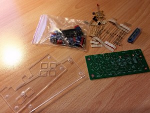
Nibbler-solderingA few days ago, the printed circuit board (PCB) for my 4-bit do-it-yourself CPU project has arrived. The next step was to get the parts together. That's a bit of a tricky thing as many components, especially the 74HC181 chip that implements the Arithmetic Logic Unit (ALU), while having been quite popular in the 1970's, are a bit on the antique side these days.

In the end, I bought the parts in 3 different stores. Most of the parts came from Digikey in the US and I was surprised how fast they delivered. I ordered on a Monday evening European time and the parts were delivered two days later on Wednesday morning. As I was ordering parts for more than 65 euros, delivery to Europe was free of charge and Digikey took care of customs procedures, taxes. etc. An incredible turn-around time, looks their logistics are quite optimized.

Other, more common parts, like most logic chips came from an electronics store in Germany with an equally impressive turn-around time. The 74HC181 ALU IC was a special case, neither Digikey nor the German electronics store had that part in stock. Thanks to Google, I was able to find the ALU at Darisus, another electronics mail delivery company in Germany that had it in stock. All parcels arrived Wednesday so I was set to go in less than two days. Quite a difference to the days when you ordered by mail and expected a response a week or two later…

The picture on the left shows my current progress. Most parts and the IC sockets are already soldered, the next step is to flash the microcode- and the program ROMs.